
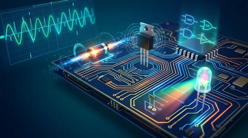
📌 اس Chapter میں Topics (Topics in this Chapter)
- 1. Semiconductors & Doping سیمی کنڈکٹرز
- 2. PN Junction & Diode Biasing پی این جنکشن ڈائیوڈ
- 3. Light-Emitting Diode (LED) ایل ای ڈی (LED)
- 4. Analogue & Digital (ADC/DAC) اینالاگ اور ڈیجیٹل
- 5. Boolean Logic & Logic Gates بولین الجبرا اور گیٹس
- 6. Burglar & Fire Alarm Circuits سیکیورٹی الارم سرکٹس
- 📝 Section A: Solved MCQs معروضی سوالات
- 📝 Section B: Short Questions مختصر سوالات
- 📝 Section C: Constructed Response فہم پر مبنی سوالات
- 📝 Section D: Long Questions تفصیلی سوالات
🔍 اس Chapter میں تلاش کرو (Instant Topic & Q&A Filter)
Quick Topic Tags (Click to filter):
19.1 Introduction to Electronics, Semiconductors & Doping
19.1 الیکٹرانکس، سیمی کنڈکٹرز اور ڈوپنگ کا تعارف
Electronics: Electronics is the branch of physics and technology that deals with the study and control of the flow of electrons in semiconductor devices and circuits.
Semiconductors: A semiconductor is a crystalline material whose electrical conductivity lies between that of a conductor (like copper) and an insulator (like glass). The most widely used semiconductors are Silicon (Si) and Germanium (Ge), which have 4 valence electrons in their outermost shell.
Doping & Extrinsic Semiconductors: Pure semiconductors have low conductivity at room temperature. Doping is the process of adding a very small, controlled amount of impurity atoms to a pure semiconductor to increase its electrical conductivity:
- N-Type Semiconductor: Formed by doping Silicon with a pentavalent impurity (Group V element having 5 valence electrons, e.g., Phosphorus, Arsenic, Antimony). Four electrons form covalent bonds and the fifth becomes a free electron. Thus, free electrons are majority carriers.
- P-Type Semiconductor: Formed by doping Silicon with a trivalent impurity (Group III element having 3 valence electrons, e.g., Boron, Aluminium, Gallium). This leaves a deficiency of one electron called a hole (positive charge carrier). Thus, holes are majority carriers.
الیکٹرانکس (Electronics): فزکس اور ٹیکنالوجی کی وہ شاخ جو آلات اور سرکٹس میں الیکٹرانز کے بہاؤ کے مطالعہ اور کنٹرول سے بحث کرتی ہے، الیکٹرانکس کہلاتی ہے۔
سیمی کنڈکٹرز (Semiconductors): سیمی کنڈکٹر ایسا مادہ ہے جس کی برقی موصلیت (electrical conductivity) کنڈکٹرز (مثلاً تانبا) اور انسولیٹرز (مثلاً شیشہ) کے درمیان ہوتی ہے۔ سب سے زیادہ استعمال ہونے والے سیمی کنڈکٹرز سلیکون (Si) اور جرمنیم (Ge) ہیں جن کے بیرونی شیل میں 4 ویلنس الیکٹرانز ہوتے ہیں۔
ڈوپنگ (Doping) اور اس کی اقسام: خالص سیمی کنڈکٹر میں کمرے کے درجہ حرارت پر برقی موصلیت کم ہوتی ہے۔ سیمی کنڈکٹر کی برقی موصلیت بڑھانے کے لیے اس میں معمولی مقدار میں کثافت (impurity) ملانے کے عمل کو ڈوپنگ کہتے ہیں:
- N-ٹائپ سیمی کنڈکٹر: جب خالص سلیکون میں پینٹا ویلنٹ کثافت (5 ویلنس الیکٹرانز والے عناصر مثلاً فاسفورس) ملائی جائے تو N-ٹائپ سیمی کنڈکٹر بنتا ہے۔ اس میں آزاد الیکٹرانز اکثریتی چارج کیریئرز ہوتے ہیں۔
- P-ٹائپ سیمی کنڈکٹر: جب خالص سلیکون میں ٹرائی ویلنٹ کثافت (3 ویلنس الیکٹرانز والے عناصر مثلاً بوران یا ایلومینیم) ملائی جائے تو الیکٹران کی کمی سے ایک خالی جگہ بنتی ہے جسے ہول (Hole) کہتے ہیں۔ اس میں ہولز اکثریتی چارج کیریئرز ہوتے ہیں۔
19.2 P-N Junction Diode, Depletion Region & Biasing
19.2 پی-این جنکشن ڈائیوڈ، ڈیپلیشن ریجن اور بائسنگ
P-N Junction & Depletion Region: When a P-type and an N-type semiconductor crystal are joined together, free electrons from the N-side diffuse across the junction and recombine with holes on the P-side. This creates a narrow charge-free zone around the junction called the depletion region.
Potential Barrier: Due to immobile positive ions on the N-side and negative ions on the P-side of the junction, a potential difference develops that stops further diffusion. At room temperature, this barrier voltage is 0.7 V for Silicon and 0.3 V for Germanium.
- Forward Bias (Conducting State): When the P-side (Anode) is connected to the positive terminal and the N-side (Cathode) to the negative terminal of a battery, the external voltage opposes the potential barrier. The depletion region narrows, and a large current flows once the battery voltage exceeds 0.7 V (Si) or 0.3 V (Ge).
- Reverse Bias (Blocking State): When the P-side is connected to the negative terminal and the N-side to the positive terminal, charge carriers are pulled away from the junction. The depletion region widens, blocking majority current. Only a tiny leakage current flows due to minority carriers.
پی-این جنکشن اور ڈیپلیشن ریجن: جب ایک P-ٹائپ اور ایک N-ٹائپ سیمی کنڈکٹر کو آپس میں جوڑا جاتا ہے تو N-حصے کے آزاد الیکٹرانز جنکشن پار کر کے P-حصے کے ہولز کے ساتھ مل جاتے ہیں، جس سے جنکشن کے گرد آزاد چارج کیریئرز سے خالی ایک علاقہ بن جاتا ہے جسے ڈیپلیشن ریجن (Depletion Region) کہتے ہیں۔
پوٹینشل بیریئر (Potential Barrier): ڈیپلیشن ریجن چارجز کی مزید حرکت کے خلاف رکاوٹ کا کام کرتا ہے۔ اسے عبور کرنے کے لیے سلیکون ڈائیوڈ کے لیے 0.7 V اور جرمنیم ڈائیوڈ کے لیے 0.3 V بیرونی وولٹیج درکار ہوتا ہے۔
- فارورڈ بائس (Forward Bias): جب ڈائیوڈ کے P-سائیڈ کو بیٹری کے مثبت (+) ٹرمینل اور N-سائیڈ کو منفی (–) ٹرمینل سے جوڑا جائے تو پوٹینشل بیریئر کم ہو جاتا ہے، ڈیپلیشن ریجن سکڑ جاتا ہے اور ڈائیوڈ میں سے آسانی سے کرنٹ گزرتا ہے۔
- ریورس بائس (Reverse Bias): جب P-سائیڈ کو بیٹری کے منفی (–) ٹرمینل اور N-سائیڈ کو مثبت (+) ٹرمینل سے جوڑا جائے تو ڈیپلیشن ریجن چوڑا ہو جاتا ہے اور اکثریتی چارجز کا بہاؤ رک جاتا ہے۔ صرف اقلیتی کیریئرز کی وجہ سے انتہائی معمولی لیکیج کرنٹ (Leakage Current) بہتا ہے۔
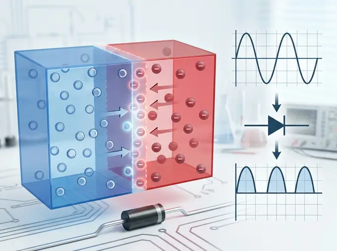
Diagram se samjho: Left تصویر میں P-N junction کے درمیان Depletion Region اور AC سے DC wave بنتے ہوئے دیکھایا گیا ہے; Right schematic میں Diode کا circuit symbol (Anode P-side triangle aur Cathode N-side vertical bar) اور Forward/Reverse bias کا فرق واضح ہے.
19.3 Light-Emitting Diode (LED) — Working & Applications
19.3 لائٹ ایمیٹنگ ڈائیوڈ (LED) — کام کرنے کا اصول اور استعمالات
What is an LED? A Light-Emitting Diode (LED) is a specialized P-N junction semiconductor diode that emits visible (or infrared) light when an electric current passes through it in forward bias.
How an LED Produces Light: When an LED is connected in forward bias, the applied voltage reduces the depletion region and electrons from the N-type region cross the junction to recombine with holes in the P-type region. During this recombination, electrons fall from a higher energy level to a lower energy level and release energy in the form of light packets called photons.
- Why LEDs Do Not Glow in Reverse Bias: In reverse bias, the depletion region widens and no majority current flows, so no recombination occurs and no light is emitted.
- What Determines LED Colour: The colour (wavelength) of light emitted by an LED depends on the type of semiconductor material (such as Gallium Arsenide Phosphide or Gallium Nitride) used in its construction, not the colour of the plastic casing.
- Uses of LEDs: Digital clocks, seven-segment calculator displays, TV remote controls, traffic signals, indicator lamps, and energy-saving home lighting.
ایل ای ڈی (LED) کیا ہے؟ لائٹ ایمیٹنگ ڈائیوڈ (LED) ایک خاص پی-این جنکشن سیمی کنڈکٹر ڈائیوڈ ہے جو فارورڈ بائس میں برقی رو گزرنے پر روشنی خارج کرتا ہے۔
ایل ای ڈی روشنی کیسے پیدا کرتا ہے؟ جب ایل ای ڈی کو فارورڈ بائس میں جوڑا جاتا ہے تو N-ٹائپ مادے سے الیکٹرانز جنکشن پار کر کے P-ٹائپ مادے کے ہولز کے ساتھ مل جاتے ہیں (Recombination)۔ اس ملاپ کے دوران توانائی روشنی کے ذرات یعنی فوٹونز (Photons) کی صورت میں خارج ہوتی ہے جس سے ایل ای ڈی روشن ہو جاتا ہے۔
- ریورس بائس میں ایل ای ڈی کیوں نہیں جلتا؟ ریورس بائس میں ڈیپلیشن ریجن چوڑا ہو جاتا ہے اور کرنٹ نہیں گزرتا، اس لیے کوئی روشنی خارج نہیں ہوتی۔
- روشنی کے رنگ کا انحصار: ایل ای ڈی سے نکلنے والی روشنی کا رنگ اس کی تیاری میں استعمال ہونے والے سیمی کنڈکٹر مادے کی قسم پر منحصر ہوتا ہے (جس سے فوٹون کی طولِ موج طے ہوتی ہے)۔
- استعمالات: ڈیجیٹل گھڑیاں، کیلکولیٹر، ٹی وی ریموٹ، ٹریفک سگنلز، سکرین ڈسپلے اور کم بجلی خرچ کرنے والے جدید بلب۔
19.4 Analogue & Digital Signals — ADC, DAC, Bit and Byte
19.4 اینالاگ اور ڈیجیٹل سگنلز — ADC، DAC، بٹ اور بائٹ
Analogue vs. Digital Circuits:
- Analogue Signals & Circuits: Signals (such as sound, temperature, and light intensity) that vary smoothly and continuously over a range of values with time.
- Digital Signals & Circuits: Signals that have only two discrete voltage levels: HIGH (Logic 1, e.g., +5 V) and LOW (Logic 0, e.g., 0 V). Digital signals are much more reliable over long distances because two distinct levels (1 and 0) are easily distinguished from electrical noise.
ADC (Analogue-to-Digital Converter): Converts real-world continuous analogue signals (e.g., microphone voice) into binary digital data (0s and 1s) in three steps:
- Sampling: Measuring the analogue signal's amplitude at regular time intervals.
- Quantization: Rounding each sampled value to the nearest predefined level.
- Encoding: Converting each quantized level into binary numbers (0s and 1s).
DAC (Digital-to-Analog Converter): Converts processed binary data (0s and 1s) back into an analogue signal (e.g., driving a loudspeaker). 1 Bit is a single binary digit (0 or 1), and 1 Byte = 8 Bits.
اینالاگ اور ڈیجیٹل سرکٹس کا فرق:
- اینالاگ سگنلز: وہ سگنلز (مثلاً آواز، درجہ حرارت، روشنی) جن کی قیمت وقت کے ساتھ مسلسل اور بتدریج تبدیل ہوتی ہے۔
- ڈیجیٹل سگنلز: وہ سگنلز جن کی صرف دو متعین سطحیں (Discrete Levels) ہوتی ہیں: ہائی (1) اور لو (0)۔ ڈیجیٹل سگنلز طویل فاصلے کی ترسیل میں زیادہ قابلِ اعتماد ہوتے ہیں کیونکہ شور (noise) کے باوجود 0 اور 1 کی پہچان آسان رہتی ہے۔
اے ڈی سی (ADC - Analogue to Digital Converter): اینالاگ سگنل کو کمپیوٹر کے سمجھنے کے لیے ڈیجیٹل بائنری شکل (0 اور 1) میں تین مراحل کے ذریعے تبدیل کرتا ہے:
- سیمپلنگ (Sampling): مقررہ وقفوں پر اینالاگ سگنل کی پیمائش کرنا۔
- کوانٹائزیشن (Quantization): ہر پیمائش کو قریبی مقررہ درجے تک راؤنڈ کرنا۔
- انکوڈنگ (Encoding): ان درجوں کو بائنری اعداد (0 اور 1) میں بدلنا۔
ڈی اے سی (DAC): بائنری ڈیٹا کو واپس اینالاگ سگنل (مثلاً سپیکر کی آواز) میں بدلتا ہے۔ کمپیوٹر میں ڈیٹا کی سب سے چھوٹی اکائی بٹ (0 یا 1) ہے اور 1 بائٹ = 8 بٹس۔
19.5 Boolean Algebra & Logic Gates (AND, OR, NOT, NAND, NOR)
19.5 بولین الجبرا اور لاجک گیٹس (AND, OR, NOT, NAND, NOR)
Boolean Algebra: Developed by George Boole, Boolean algebra is the mathematics of binary variables having only two states: TRUE (1 / High) and FALSE (0 / Low). It uses three basic operations: AND, OR, and NOT.
Logic Gates: Electronic digital circuits that perform Boolean logic operations on one or more binary inputs to produce a single binary output:
- AND Gate (X = A · B): Output is 1 ONLY when both inputs A and B are 1.
- OR Gate (X = A + B): Output is 1 when at least one input (A or B) is 1; output is 0 only when both are 0.
- NOT Gate / Inverter (X = Ā): Has a single input and inverts it: if input is 1, output is 0; if input is 0, output is 1.
- NAND Gate (X = A · B): Combination of AND followed by NOT. Output is 0 ONLY when both inputs A and B are 1; otherwise output is 1.
- NOR Gate (X = A + B): Combination of OR followed by NOT. Output is 1 ONLY when both inputs A and B are 0; otherwise output is 0. Both NAND and NOR are Universal Gates because any other gate can be constructed from them.
بولین الجبرا (Boolean Algebra): جارج بول (George Boole) نے بولین الجبرا متعارف کرایا جو ڈیجیٹل الیکٹرانکس اور کمپیوٹنگ کی بنیاد ہے۔ اس میں متغیرات کی صرف دو ممکنہ قیمتیں ہوتی ہیں: 1 (ہائی/درست) یا 0 (لو/غلط)۔
لاجک گیٹس (Logic Gates): وہ بنیادی ڈیجیٹل سرکٹس جو بائنری ان پٹس پر منطقی عوامل (Logical Operations) سرانجام دیتے ہیں:
- AND گیٹ (X = A · B): آؤٹ پٹ صرف اس وقت 1 ہوتی ہے جب دونوں ان پٹس A اور B کی قیمت 1 ہو۔
- OR گیٹ (X = A + B): اگر کم از کم ایک ان پٹ بھی 1 ہو تو آؤٹ پٹ 1 ہوتی ہے؛ آؤٹ پٹ صرف تب 0 ہوتی ہے جب دونوں ان پٹس 0 ہوں۔
- NOT گیٹ / انورٹر (X = Ā): اس کی ایک ہی ان پٹ ہوتی ہے اور یہ سگنل کو الٹ دیتا ہے (0 کو 1 اور 1 کو 0 کر دیتا ہے)۔
- NAND گیٹ (X = A · B): یہ AND اور NOT کا مجموعہ ہے۔ آؤٹ پٹ صرف تب 0 ہوتی ہے جب دونوں ان پٹس 1 ہوں، ورنہ 1 رہتی ہے۔
- NOR گیٹ (X = A + B): یہ OR اور NOT کا مجموعہ ہے۔ آؤٹ پٹ صرف تب 1 ہوتی ہے جب دونوں ان پٹس 0 ہوں۔ NAND اور NOR کو یونیورسل گیٹس کہتے ہیں۔
1. AND Gate X = A · B
Output is HIGH (1) only when all inputs are HIGH (1).
| Input A | Input B | Output X = A · B |
|---|---|---|
| 0 | 0 | 0 |
| 0 | 1 | 0 |
| 1 | 0 | 0 |
| 1 | 1 | 1 |
2. OR Gate X = A + B
Output is HIGH (1) when any input is HIGH (1).
| Input A | Input B | Output X = A + B |
|---|---|---|
| 0 | 0 | 0 |
| 0 | 1 | 1 |
| 1 | 0 | 1 |
| 1 | 1 | 1 |
3. NOT Gate (Inverter) X = Ā
Single-input gate that reverses (inverts) the input state.
| Input A | Output X = Ā |
|---|---|
| 0 | 1 |
| 1 | 0 |
4. NAND Gate (Universal) X = A · B
Output is LOW (0) only when both inputs are HIGH (1).
| Input A | Input B | Output X = A · B |
|---|---|---|
| 0 | 0 | 1 |
| 0 | 1 | 1 |
| 1 | 0 | 1 |
| 1 | 1 | 0 |
5. NOR Gate (Universal) X = A + B
Output is HIGH (1) only when both inputs are LOW (0).
| Input A | Input B | Output X = A + B |
|---|---|---|
| 0 | 0 | 1 |
| 0 | 1 | 0 |
| 1 | 0 | 0 |
| 1 | 1 | 0 |

یاد رکھنے کی آسان trick: AND تب 1 دیتا ہے جب dono 1 hon; NAND اسکا الٹا ہے (تب 0 دیتا ہے جب dono 1 hon). OR تب 0 دیتا ہے جب dono 0 hon; NOR اسکا الٹا ہے (صرف تب 1 دیتا ہے جب dono 0 hon)!
19.6 Practical Applications: Burglar Alarm (NAND Gate) & Fire Alarm (OR Gate)
19.6 عملی اطلاقیے: برگلر الارم (NAND گیٹ) اور فائر الارم (OR گیٹ)
1. Burglar Alarm Using a NAND Gate & LDR:
- Components: A single NAND gate, an LDR (Light-Dependent Resistor) at input B, a push-button switch (S) at input A, and an alarm buzzer at output X.
- Normal Standby State (A = 1, B = 1 → X = 0): When light falls continuously on the LDR, its resistance is low and input B stays HIGH (1). When the switch S is untouched, input A stays HIGH (1). Since both inputs are 1, the NAND gate outputs 0 (Alarm OFF).
- Intruder Triggered State (X = 1): If a burglar blocks the light beam (LDR resistance increases → B = 0) OR steps on the hidden switch (A = 0), at least one input becomes 0. The NAND gate immediately outputs 1 (HIGH), sounding the alarm!
2. Fire Alarm System Using an OR Gate:
- Uses a smoke sensor (Input A) and a heat sensor (Input B) connected to an OR gate. If either smoke (A = 1) OR excessive heat (B = 1) is detected, the OR gate outputs 1 and triggers the fire alarm early to save lives.
1. NAND گیٹ اور LDR کے ذریعے برگلر الارم (چوری روکنے والا الارم):
- بناوٹ: اس سرکٹ میں ایک NAND گیٹ، ایک LDR (روشنی پر منحصر رزسٹر) ان پٹ B پر، ایک پش بٹن سوئچ (S) ان پٹ A پر، اور آؤٹ پٹ X پر الارم لگایا جاتا ہے۔
- عام حالت (A = 1, B = 1 ← X = 0): جب LDR پر روشنی پڑ رہی ہو تو اس کی مزاحمت کم ہوتی ہے اور ان پٹ B ہائی (1) رہتی ہے، اور جب سوئچ S نہ دبا ہو تو ان پٹ A بھی ہائی (1) رہتی ہے۔ دونوں ان پٹس 1 ہونے کی وجہ سے NAND گیٹ کی آؤٹ پٹ 0 (الارم بند) رہتی ہے۔
- خطرے کی حالت (X = 1): اگر چور روشنی کا راستہ روکے (B = 0) یا سوئچ پر پاؤں رکھ دے (A = 0)، تو NAND گیٹ کی آؤٹ پٹ فوراً 1 (ہائی) ہو جاتی ہے اور الارم بج اٹھتا ہے۔
2. OR گیٹ کے ذریعے فائر الارم سسٹم:
- فائر الارم میں دھوئیں کے سینسر (A) اور حرارت کے سینسر (B) کو OR گیٹ سے جوڑا جاتا ہے تاکہ دھواں یا حرارت میں سے کوئی ایک بھی محسوس ہو تو آؤٹ پٹ 1 ہو جائے اور الارم بج جائے۔
1. (Textbook Exercise 19.1) A semiconductor diode allows electric current to flow in:
1. ایک سیمی کنڈکٹر ڈائیوڈ برقی رو (کرنٹ) کو بہنے دیتا ہے:
Show Answer & Explanation / جواب اور وضاحت ▼
✅ Correct Answer: (C) One direction only (صرف ایک سمت میں)
Explanation: A P-N junction diode acts like a one-way valve: it conducts current only in forward bias and blocks current in reverse bias.
اردو Wazahat: Diode current کے لیے one-way road کی طرح کام کرتا ہے — صرف forward bias میں current گزرنے دیتا ہے.
2. (Textbook Exercise 19.2) What is the primary function of a Light-Emitting Diode (LED)?
2. لائٹ ایمیٹنگ ڈائیوڈ (LED) کا بنیادی کام کیا ہے؟
Show Answer & Explanation / جواب اور وضاحت ▼
✅ Correct Answer: (B) To emit light when current passes in one direction
Explanation: An LED is a forward-biased P-N junction diode that emits visible light photons when electrons recombine with holes.
3. (Textbook Exercise 19.3) The output of a two-input NOR gate is '1' (HIGH) when:
3. دو ان پٹ والے NOR گیٹ کی آؤٹ پٹ '1' کب ہوتی ہے؟
Show Answer & Explanation / جواب اور وضاحت ▼
✅ Correct Answer: (C) Both A and B are '0'
Explanation: For a NOR gate (X = A + B), when A = 0 and B = 0, A + B = 0, and inverting it gives X = 1.
4. (Textbook Exercise 19.4) The output of a NAND gate is '0' (LOW) when:
4. ایک NAND گیٹ کی آؤٹ پٹ '0' کب ہوتی ہے؟
Show Answer & Explanation / جواب اور وضاحت ▼
✅ Correct Answer: (B) Both of its inputs are '1'
Explanation: A NAND gate (X = A · B) inverts the AND output, so it outputs 0 only when A = 1 and B = 1.
5. (Textbook Exercise 19.5) How many bits make up one byte in digital electronics and computing?
5. ڈیجیٹل الیکٹرانکس اور کمپیوٹنگ میں کتنے بٹس مل کر ایک بائٹ (Byte) بناتے ہیں؟
Show Answer & Explanation / جواب اور وضاحت ▼
✅ Correct Answer: (D) 8 bits
Explanation: 1 Byte = 8 bits, where each bit is a binary digit having value 0 or 1.
6. What is the approximate potential barrier voltage for a Silicon (Si) P-N junction diode at room temperature?
6. سلیکون (Si) ڈائیوڈ کے لیے پوٹینشل بیریئر وولٹیج کی مقدار تقریباً کتنی ہوتی ہے؟
Show Answer & Explanation / جواب اور وضاحت ▼
✅ Correct Answer: (A) 0.7 V
Explanation: For Silicon (Si) diodes the barrier potential is 0.7 V, whereas for Germanium (Ge) diodes it is 0.3 V.
7. Adding a pentavalent impurity (like Phosphorus) to pure Silicon produces:
7. خالص سلیکون میں پینٹا ویلنٹ کثافت (مثلاً فاسفورس) ملانے سے بنتا ہے:
Show Answer & Explanation / جواب اور وضاحت ▼
✅ Correct Answer: (B) N-type semiconductor
Explanation: Pentavalent atoms have 5 valence electrons; 4 form covalent bonds and the 5th becomes a free negative electron, creating an N-type semiconductor.
8. What is the correct sequence of the three steps in an Analogue-to-Digital Converter (ADC)?
8. اینالاگ سے ڈیجیٹل تبدیلی (ADC) کے تین مراحل کی درست ترتیب کیا ہے؟
Show Answer & Explanation / جواب اور وضاحت ▼
✅ Correct Answer: (C) Sampling → Quantization → Encoding
Explanation: First the analogue signal is sampled at regular intervals, then quantized to nearest levels, and finally encoded into binary 0s and 1s.
9. Which logic gate is also known as an inverter?
9. کس لاجک گیٹ کو انورٹر (Inverter) بھی کہا جاتا ہے؟
Show Answer & Explanation / جواب اور وضاحت ▼
✅ Correct Answer: (A) NOT gate
Explanation: A NOT gate has one input and reverses (inverts) the binary state from 0 to 1 and from 1 to 0.
10. Which logic gate is used in a fire alarm system that triggers when EITHER smoke OR heat is detected?
10. فائر الارم سسٹم میں کون سا گیٹ استعمال ہوتا ہے جو دھواں یا حرارت میں سے کسی ایک کی موجودگی پر بھی الارم چلا دیتا ہے؟
Show Answer & Explanation / جواب اور وضاحت ▼
✅ Correct Answer: (D) OR gate
Explanation: An OR gate outputs HIGH (1) when either input A (smoke) or input B (heat) or both are HIGH (1).
► Q1. Define electronics and semiconductor. Give two examples of semiconductors. الیکٹرانکس اور سیمی کنڈکٹر کی تعریف کریں۔
Answer (English): Electronics is the branch of physics that deals with the study and control of the flow of electrons in devices and circuits. A semiconductor is a material whose electrical conductivity lies between that of conductors and insulators. Examples: Silicon (Si) and Germanium (Ge).
جواب (اردو): الیکٹرانکس سائنس کی وہ شاخ ہے جو آلات اور سرکٹس میں الیکٹرانز کے بہاؤ اور کنٹرول سے بحث کرتی ہے۔ سیمی کنڈکٹر وہ مادہ ہے جس کی برقی موصلیت کنڈکٹرز اور انسولیٹرز کے درمیان ہوتی ہے، مثلاً سلیکون (Si) اور جرمنیم (Ge)۔
► Q2. What is doping? Differentiate between N-type and P-type semiconductors. ڈوپنگ کیا ہے؟ N-ٹائپ اور P-ٹائپ سیمی کنڈکٹر میں فرق لکھیں۔
Answer (English): Doping is the process of adding a small amount of impurity to a pure semiconductor to increase its electrical conductivity. N-type semiconductor is formed by adding a pentavalent impurity (e.g., Phosphorus) and has free electrons as majority carriers. P-type semiconductor is formed by adding a trivalent impurity (e.g., Boron) and has holes as majority carriers.
جواب (اردو): خالص سیمی کنڈکٹر کی برقی موصلیت بڑھانے کے لیے اس میں معمولی مقدار میں کثافت (impurity) ملانے کے عمل کو ڈوپنگ کہتے ہیں۔ پینٹا ویلنٹ کثافت (مثلاً فاسفورس) ملانے سے N-ٹائپ سیمی کنڈکٹر بنتا ہے جس میں آزاد الیکٹرانز اکثریتی چارج کیریئرز ہوتے ہیں، جبکہ ٹرائی ویلنٹ کثافت (مثلاً بوران) ملانے سے P-ٹائپ سیمی کنڈکٹر بنتا ہے جس میں ہولز (Holes) اکثریتی چارج کیریئرز ہوتے ہیں۔
► Q3. What is a P-N junction and how is the depletion region formed? پی-این جنکشن کیا ہے اور ڈیپلیشن ریجن کیسے بنتا ہے؟
Answer (English): When an N-type and a P-type semiconductor are joined together, they form a PN junction. Immediately after joining, free electrons from the N-side diffuse across the junction and recombine with holes on the P-side, creating a region devoid of free charge carriers called the depletion region.
جواب (اردو): جب N-ٹائپ اور P-ٹائپ سیمی کنڈکٹر کو ملایا جاتا ہے تو پی-این جنکشن بنتا ہے۔ ملاپ کے فوراً بعد N-سائیڈ کے الیکٹرانز جنکشن پار کر کے P-سائیڈ کے ہولز سے مل جاتے ہیں، جس سے جنکشن کے گرد آزاد چارج کیریئرز سے خالی ایک علاقہ بن جاتا ہے جسے ڈیپلیشن ریجن کہتے ہیں۔
► Q4. Why is external voltage applied to a PN junction diode? State the barrier voltage for Silicon and Germanium. پی-این جنکشن ڈائیوڈ کو بیرونی وولٹیج کیوں دیا جاتا ہے؟ سلیکون اور جرمنیم کا بیریئر وولٹیج لکھیں۔
Answer (English): The depletion region acts as a potential barrier that prevents further movement of charges across the junction. An external voltage is applied to overcome this barrier so current can flow. The required barrier voltage is about 0.7 V for Silicon and 0.3 V for Germanium.
جواب (اردو): ڈیپلیشن ریجن چارجز کے مزید بہاؤ کے خلاف ایک رکاوٹ (پوٹینشل بیریئر) کا کام کرتا ہے۔ اس رکاوٹ کو ختم کر کے کرنٹ گزارنے کے لیے بیرونی وولٹیج لگایا جاتا ہے۔ سلیکون ڈائیوڈ کے لیے یہ وولٹیج تقریباً 0.7 V اور جرمنیم کے لیے 0.3 V ہوتا ہے۔
► Q5. Differentiate between forward bias and reverse bias of a semiconductor diode. ڈائیوڈ کی فارورڈ بائس اور ریورس بائس حالت میں فرق بیان کریں۔
Answer (English): In forward bias, the P-side is connected to the positive terminal and the N-side to the negative terminal of a battery; the depletion region narrows and a large current flows. In reverse bias, the P-side is connected to the negative terminal and the N-side to the positive terminal; the depletion region widens and blocks majority current flow.
جواب (اردو): فارورڈ بائس میں P-سائیڈ کو بیٹری کے مثبت (+) اور N-سائیڈ کو منفی (–) ٹرمینل سے جوڑا جاتا ہے جس سے ڈیپلیشن ریجن پتلا ہو جاتا ہے اور کرنٹ بہتا ہے۔ ریورس بائس میں P-سائیڈ کو منفی (–) اور N-سائیڈ کو مثبت (+) ٹرمینل سے جوڑا جاتا ہے جس سے ڈیپلیشن ریجن چوڑا ہو جاتا ہے اور کرنٹ رک جاتا ہے۔
► Q6. What is leakage current in a diode? ڈائیوڈ میں لیکیج کرنٹ (Leakage Current) سے کیا مراد ہے؟
Answer (English): Leakage current is the very small current that flows through a P-N junction diode when it is connected in reverse bias, caused by the movement of thermally generated minority charge carriers across the junction.
جواب (اردو): ریورس بائس حالت میں اقلیتی چارج کیریئرز (minority carriers) کی حرکت کی وجہ سے ڈائیوڈ میں جو انتہائی معمولی کرنٹ بہتا ہے، اسے لیکیج کرنٹ کہتے ہیں۔
► Q7. What is an LED and why does it work only in forward bias? ایل ای ڈی (LED) کیا ہے اور یہ صرف فارورڈ بائس میں ہی کیوں کام کرتا ہے؟
Answer (English): A Light-Emitting Diode (LED) is a semiconductor diode that emits light when electric current passes through it. It works only in forward bias because charge carriers cross the junction and recombine to emit photons only in forward bias; in reverse bias, the depletion region widens and prevents current flow, so no light is emitted.
جواب (اردو): ایل ای ڈی ایک ایسا سیمی کنڈکٹر ڈائیوڈ ہے جو کرنٹ گزرنے پر روشنی خارج کرتا ہے۔ یہ صرف فارورڈ بائس میں کام کرتا ہے کیونکہ فارورڈ بائس ہی میں الیکٹرانز اور ہولز جنکشن پار کر کے آپس میں ملتے ہیں اور فوٹونز خارج کرتے ہیں، جبکہ ریورس بائس میں کرنٹ بند ہونے کی وجہ سے روشنی پیدا نہیں ہوتی۔
► Q8. Write any four practical uses/advantages of LEDs. ایل ای ڈی (LED) کے چار فوائد اور استعمالات لکھیں۔
Answer (English): LEDs are energy-saving, long-lasting, durable, and fast-switching. They are widely used in: (1) Digital clocks and calculators, (2) TV remote controls, (3) Traffic signals and vehicle brake lights, and (4) Modern home and street lighting.
جواب (اردو): ایل ای ڈی کم بجلی خرچ کرنے والے، پائیدار اور طویل عمر رکھنے والے آلات ہیں۔ ان کے چار اہم استعمالات یہ ہیں: (1) ڈیجیٹل گھڑیاں اور کیلکولیٹر، (2) ٹی وی ریموٹ کنٹرول، (3) ٹریفک سگنلز، اور (4) گھروں اور سڑکوں کی جدید لائٹنگ۔
► Q9. Differentiate between analogue circuits and digital circuits. اینالاگ سرکٹس اور ڈیجیٹل سرکٹس میں فرق بیان کریں۔
Answer (English): In analogue circuits, voltages and currents vary smoothly and continuously over a range of values. In digital circuits, voltages have only two discrete values: "HIGH" (Logic 1, e.g., 5 V) or "LOW" (Logic 0, e.g., 0 V).
جواب (اردو): اینالاگ سرکٹس میں وولٹیج اور کرنٹ ایک خاص حد کے اندر مسلسل اور بتدریج تبدیل ہوتے ہیں، جبکہ ڈیجیٹل سرکٹس میں وولٹیج کی صرف دو متعین قیمتیں ہوتی ہیں: "ہائی" (1) یا "لو" (0)۔
► Q10. What is an ADC and what are its three conversion steps? اے ڈی سی (ADC) کیا ہے اور اس کے تین مراحل کون سے ہیں؟
Answer (English): An Analogue-to-Digital Converter (ADC) converts continuous analogue signals (like sound or light) into digital binary data (0s and 1s) for processing by computers. Its three steps are: (1) Sampling, (2) Quantization, and (3) Encoding.
جواب (اردو): اینالاگ ٹو ڈیجیٹل کنورٹر (ADC) اینالاگ سگنلز (مثلاً آواز) کو کمپیوٹر کے لیے بائنری ڈیجیٹل ڈیٹا (0 اور 1) میں تبدیل کرتا ہے۔ اس کے تین مراحل ہیں: (1) سیمپلنگ (Sampling)، (2) کوانٹائزیشن (Quantization)، اور (3) انکوڈنگ (Encoding)۔
► Q11. What is a DAC? Give an example of its use. ڈی اے سی (DAC) کیا ہے؟ اس کے استعمال کی مثال دیں۔
Answer (English): A Digital-to-Analogue Converter (DAC) converts binary digital data (0s and 1s) back into a continuous analogue signal for output — for example, converting digital audio files in a mobile phone into analogue electrical signals to drive a loudspeaker.
جواب (اردو): ڈیجیٹل ٹو اینالاگ کنورٹر (DAC) بائنری ڈیٹا (0 اور 1) کو واپس اینالاگ سگنل میں تبدیل کرتا ہے، مثلاً موبائل فون یا کمپیوٹر میں ڈیجیٹل آڈیو کو سپیکر سے سنانے کے لیے اینالاگ سگنل میں بدلنا۔
► Q12. Define Boolean algebra, bit, and byte. بولین الجبرا، بٹ (Bit) اور بائٹ (Byte) کی تعریف کریں۔
Answer (English): Boolean algebra (developed by George Boole) is the algebra of binary variables having only two values: 0 and 1. A bit is the smallest unit of data in computing (either 0 or 1). A byte is a group of 8 bits.
جواب (اردو): بولین الجبرا (جسے جارج بول نے پیش کیا) بائنری متغیرات (0 اور 1) کا الجبرا ہے جو ڈیجیٹل سرکٹس کی بنیاد ہے۔ کمپیوٹنگ میں ڈیٹا کی سب سے چھوٹی اکائی بٹ (0 یا 1) ہے، اور 8 بٹس کے مجموعے کو بائٹ (Byte) کہتے ہیں۔
► Q13. What is a logic gate? Name the three basic Boolean logic operations. لاجک گیٹ کیا ہے؟ تین بنیادی بولین لاجک عوامل کے نام لکھیں۔
Answer (English): A logic gate is a basic building block of digital circuits that performs a logical operation on binary inputs to produce a binary output. The three basic Boolean logic operations are AND, OR, and NOT.
جواب (اردو): لاجک گیٹ ڈیجیٹل سرکٹس کا بنیادی جزو ہے جو بائنری ڈیٹا پر منطقی عمل کر کے فیصلہ کرتا ہے۔ تین بنیادی بولین عوامل AND، OR اور NOT ہیں۔
► Q14. Write the logic equations of AND, OR, NOT, NAND, and NOR gates. AND، OR، NOT، NAND اور NOR گیٹس کی لاجک مساواتیں لکھیں۔
Answer (English & Urdu):
- AND Gate: X = A · B
- OR Gate: X = A + B
- NOT Gate: X = Ā
- NAND Gate: X = A · B
- NOR Gate: X = A + B
► Q15. Which logic gate is used in a fire alarm system and why? فائر الارم سسٹم میں کون سا لاجک گیٹ استعمال ہوتا ہے اور کیوں؟
Answer (English): An OR gate is used in a fire alarm system because it triggers the alarm (X = 1) when either the smoke sensor (A = 1) or the heat sensor (B = 1) detects fire.
جواب (اردو): فائر الارم سسٹم میں OR گیٹ استعمال ہوتا ہے کیونکہ اگر دھوئیں کا سینسر یا حرارت کا سینسر، دونوں میں سے کوئی ایک بھی آگ کی نشاندہی کرے تو OR گیٹ آؤٹ پٹ 1 دے کر الارم بجا دیتا ہے۔
► CRQ 19.1: Why would a diode be damaged if it is connected in reverse bias with a very high voltage? What does this tell us about the diode's physical limits?
Answer (English): A very high reverse voltage causes electrical breakdown (avalanche/Zener breakdown) across the junction, resulting in a sudden large reverse current that overheats and damages the diode. This shows that every diode has a physical limit called the Peak Inverse Voltage (breakdown voltage) that it can safely withstand in reverse bias.
جواب (اردو): ریورس بائس میں بہت زیادہ وولٹیج دینے سے جنکشن کا بریک ڈاؤن ہو جاتا ہے اور اچانک تیز کرنٹ گزرنے سے ڈائیوڈ جل کر خراب ہو جاتا ہے۔ اس سے معلوم ہوتا ہے کہ ہر ڈائیوڈ کی ریورس وولٹیج برداشت کرنے کی ایک مخصوص طبعی حد (Breakdown Limit) ہوتی ہے۔
► CRQ 19.2: What makes an LED glow brighter or dimmer depending on the voltage applied? How is this property used in adjustable display brightness?
Answer (English): As the forward voltage increases beyond the threshold voltage, the forward current through the LED increases sharply. A larger current causes more electrons and holes to recombine per second, emitting more photons and making the LED glow brighter. Display screens use this property by regulating the current/voltage to adjust screen brightness.
جواب (اردو): جب فارورڈ وولٹیج کو تھریش ہولڈ وولٹیج سے بڑھایا جاتا ہے تو ایل ای ڈی میں سے گزرنے والا کرنٹ تیزی سے بڑھتا ہے، جس سے فی سیکنڈ زیادہ الیکٹرانز اور ہولز ملتے ہیں اور زیادہ فوٹونز خارج ہونے سے روشنی تیز ہو جاتی ہے۔ موبائل اور سکرین ڈسپلے میں کرنٹ کم یا زیادہ کر کے اسی اصول کے تحت چمک (Brightness) کنٹرول کی جاتی ہے۔
► CRQ 19.3: Why are digital systems more reliable than analogue systems when transmitting signals over long distances?
Answer (English): Digital signals have only two discrete states — HIGH (1) and LOW (0) — so even if electrical noise distorts the wave slightly during long-distance transmission, the receiver can still easily distinguish between 1 and 0 and regenerate a clean signal without loss of information.
جواب (اردو): ڈیجیٹل سگنلز کی صرف دو واضح سطحیں (0 اور 1) ہوتی ہیں، اس لیے طویل فاصلے تک ترسیل کے دوران اگر نوائز (شور) شامل ہو بھی جائے تو وصول کنندہ آسانی سے 0 اور 1 میں فرق کر لیتا ہے اور معلومات ضائع نہیں ہوتیں۔
► CRQ 19.4: Why is the NOT gate also called an inverter, and how can such a simple function have a major role in digital decision-making?
Answer (English): A NOT gate is called an inverter because it reverses its input logic state (1 becomes 0, and 0 becomes 1). This operation is vital in digital decision-making because it allows circuits to trigger actions when a condition is not met (e.g., turning ON a streetlight when daylight is 0) and combines with AND/OR gates to form universal NAND and NOR gates.
جواب (اردو): NOT گیٹ کو انورٹر اس لیے کہتے ہیں کیونکہ یہ ان پٹ کو الٹ دیتا ہے (1 کو 0 اور 0 کو 1 بنا دیتا ہے)۔ ڈیجیٹل فیصلہ سازی میں اس کا کردار بہت اہم ہے کیونکہ یہ کسی شرط کے نہ ہونے پر خودکار عمل چلانے (مثلاً روشنی 0 ہونے پر سٹریٹ لائٹ 1 یعنی آن کرنے) اور NAND و NOR گیٹس بنانے کے کام آتا ہے۔
► CRQ 19.5: Why would a security system use NAND gates instead of OR or AND gates for certain logical conditions?
Answer (English): A NAND gate outputs 0 only when all security sensors are intact (both inputs HIGH = 1), and outputs 1 (activating the alarm) whenever any single sensor condition fails (becomes 0). This fail-safe behaviour makes NAND gates ideal for burglar and security alarms.
جواب (اردو): NAND گیٹ صرف اس وقت 0 دیتا ہے جب تمام حفاظتی سینسرز نارمل یعنی 1 ہوں، اور جیسے ہی کوئی ایک سینسر بھی منقطع ہو کر 0 ہوتا ہے تو NAND گیٹ فوراً 1 دے کر الارم بجا دیتا ہے۔ اسی لیے سیکیورٹی سسٹمز میں NAND گیٹ استعمال کیا جاتا ہے۔
► Long Q 19.1: Explain how the depletion region of a diode changes in forward and reverse bias. What effect does this have on current flow?
Answer (English):
- Effect of Forward Bias: When the P-side of a PN junction diode is connected to the positive terminal and the N-side to the negative terminal of a battery, the applied voltage opposes the internal potential barrier. As a result, the depletion region narrows and the barrier height decreases. Once the external voltage exceeds 0.7 V (for Silicon) or 0.3 V (for Germanium), majority carriers easily cross the junction and a large forward current flows.
- Effect of Reverse Bias: When the P-side is connected to the negative terminal and the N-side to the positive terminal of a battery, electrons and holes are pulled away from the junction. Consequently, the depletion region widens and the potential barrier increases, blocking the flow of majority carriers. Only a negligible leakage current flows due to minority carriers.
جواب (اردو): فارورڈ بائس کا اثر: جب ڈائیوڈ کے P-سائیڈ کو بیٹری کے مثبت (+) ٹرمینل اور N-سائیڈ کو منفی (–) ٹرمینل سے جوڑا جاتا ہے تو بیرونی وولٹیج پوٹینشل بیریئر کو کم کر دیتا ہے جس سے ڈیپلیشن ریجن سکڑ کر پتلا ہو جاتا ہے اور چارج کیریئرز جنکشن پار کر کے نمایاں کرنٹ پیدا کرتے ہیں۔ ریورس بائس کا اثر: جب P-سائیڈ کو منفی (–) اور N-سائیڈ کو مثبت (+) ٹرمینل سے جوڑا جاتا ہے تو چارجز جنکشن سے دور کھنچ جاتے ہیں، ڈیپلیشن ریجن چوڑا ہو جاتا ہے اور اکثریتی کرنٹ کا بہاؤ رک جاتا ہے (صرف اقلیتی کیریئرز کی وجہ سے معمولی لیکیج کرنٹ بہتا ہے)۔
► Long Q 19.2: Describe how an LED produces light. Also explain how the type of semiconductor material affects the colour of the light.
Answer (English):
- Light Production in an LED: When a Light-Emitting Diode (LED) is connected in forward bias, the applied voltage narrows the depletion region and allows free electrons from the N-region to cross the junction into the P-region. When these free electrons recombine with holes in the P-region, they transition from a higher energy state to a lower energy state, releasing the excess energy directly in the form of light photons (electroluminescence).
- Role of Semiconductor Material in Colour: The colour of emitted light depends on the wavelength (or frequency) of the photons, which is determined by the energy band gap of the semiconductor compound used during manufacture (such as Gallium Arsenide Phosphide for red/amber/yellow or Gallium Indium Nitride for blue/green).
جواب (اردو): ایل ای ڈی میں روشنی کی پیداوار: جب ایل ای ڈی کو فارورڈ بائس میں جوڑا جاتا ہے تو ڈیپلیشن ریجن کم ہو جاتا ہے اور N-ٹائپ مادے سے آزاد الیکٹرانز جنکشن پار کر کے P-ٹائپ مادے کے ہولز کے ساتھ مل جاتے ہیں۔ اس ملاپ (Recombination) کے دوران توانائی فوٹونز کی شکل میں خارج ہوتی ہے جو ہمیں روشنی کی صورت میں نظر آتی ہے۔ سیمی کنڈکٹر مادے کا رنگ پر اثر: خارج ہونے والی روشنی کا رنگ فوٹون کی طولِ موج (wavelength) پر منحصر ہوتا ہے جس کا تعین ایل ای ڈی کی تیاری میں استعمال ہونے والے سیمی کنڈکٹر مرکب کے انرجی گیپ سے ہوتا ہے۔
► Long Q 19.3: What is Boolean logic? Discuss its importance in solving complex digital problems with examples.
Answer (English):
- Boolean Logic: Introduced by George Boole, Boolean logic is a mathematical system built around binary variables that can take only two values: 1 (TRUE / HIGH) and 0 (FALSE / LOW). Its three fundamental operations are AND, OR, and NOT.
- Importance in Digital Systems: Boolean logic is physically implemented using electronic logic gates. By combining basic gates, engineers can design complex digital circuits such as computer processors (CPUs), memory chips, calculators, automated industrial controllers, and safety alarms. For example, an automated ATM verifies both card validity AND PIN correctness (AND logic), while a fire alarm triggers on smoke OR heat (OR logic).
جواب (اردو): بولین لاجک: جارج بول کا پیش کردہ بولین الجبرا ڈیجیٹل الیکٹرانکس کی بنیاد ہے جس میں متغیرات کی صرف دو قیمتیں (0 اور 1) ہوتی ہیں اور تین بنیادی عوامل (AND، OR، NOT) استعمال ہوتے ہیں۔ اہمیت: بولین لاجک کو لاجک گیٹس کے ذریعے عملی شکل دی جاتی ہے۔ ان سادہ گیٹس کو ملا کر کمپیوٹر پروسیسرز، میموری سرکٹس، کیلکولیٹرز اور خودکار سیکیورٹی سسٹمز بنائے جاتے ہیں۔
► Long Q 19.4: What are logic gates? Describe the working of NAND and OR gates with the help of truth tables and equations.
Answer (English): Logic Gates are digital electronic circuits that perform Boolean logic operations on binary inputs to produce a single binary output.
- NAND Gate (X = A · B): A combination of an AND gate followed by a NOT gate. Its output is 0 (LOW) only when both inputs A and B are 1 (HIGH); for all other input combinations (00, 01, 10), its output is 1 (HIGH).
- OR Gate (X = A + B): A two-input gate whose output is 1 (HIGH) whenever at least one of its inputs is 1 (HIGH) (01, 10, 11), and 0 (LOW) only when both inputs are 0 (00).
جواب (اردو): لاجک گیٹس وہ ڈیجیٹل سرکٹس ہیں جو بائنری ان پٹس پر منطقی عوامل سرانجام دیتے ہیں۔ NAND گیٹ (X = A · B): یہ AND اور NOT گیٹ کا مجموعہ ہے جس کی آؤٹ پٹ صرف اس وقت 0 ہوتی ہے جب دونوں ان پٹس 1 ہوں، ورنہ آؤٹ پٹ 1 ہوتی ہے۔ OR گیٹ (X = A + B): اس کی آؤٹ پٹ صرف تب 0 ہوتی ہے جب دونوں ان پٹس 0 ہوں، اور اگر کوئی ایک ان پٹ بھی 1 ہو تو آؤٹ پٹ 1 ہوتی ہے۔ (ان کے ٹروتھ ٹیبل اوپر سیکشن 19.5 میں درج ہیں)۔
► Long Q 19.5: How does a NOR gate work, and how can it be used to build other basic logic gates?
Answer (English):
- Working of NOR Gate (X = A + B): A NOR gate is an OR gate followed by a NOT gate. Its output is 1 (HIGH) ONLY when both inputs A and B are 0 (LOW); if either or both inputs are 1, the output is 0 (LOW).
- Building Other Gates Using NOR (Universal Gate):
1. NOT Gate from NOR: Tie both inputs of a NOR gate together (A = B). Then X = A + A = Ā.
2. OR Gate from NOR: Feed the output of a NOR gate into a second NOR gate wired as a NOT gate. Double inversion restores X = A + B.
3. AND Gate from NOR: Invert inputs A and B separately using two NOR-inverters, and feed their outputs into a third NOR gate (X = Ā + B̄ = A · B).
جواب (اردو): NOR گیٹ کا کام (X = A + B): یہ OR اور NOT گیٹ کا مجموعہ ہے جس کی آؤٹ پٹ صرف تب 1 ہوتی ہے جب دونوں ان پٹس A اور B صفر (0) ہوں۔ NOR گیٹ سے دیگر بنیادی گیٹس بنانا: (1) NOT گیٹ: NOR گیٹ کی دونوں ان پٹس کو آپس میں جوڑ کر ایک ہی سگنل دیں تو وہ NOT گیٹ بن جاتا ہے۔ (2) OR گیٹ: ایک NOR گیٹ کی آؤٹ پٹ کے آگے NOT کے طور پر جڑا دوسرا NOR گیٹ لگا دیں تو OR گیٹ بن جاتا ہے۔ (3) AND گیٹ: دونوں ان پٹس کو الگ الگ NOR انورٹرز سے گزار کر تیسرے NOR گیٹ میں دیں تو AND گیٹ حاصل ہوتا ہے۔
► Long Q 19.6: How can a burglar alarm be designed using a NAND gate and an LDR? Explain.
Answer (English):
- Circuit Design: A burglar alarm is built using a single NAND gate, an LDR (Light-Dependent Resistor) connected to input B, a push-button switch (S) connected to input A, and an alarm bell/siren at output X.
- Working in Normal Condition: When a continuous light beam falls on the LDR, its resistance remains low, keeping input B = 1 (HIGH). When the push-button switch S is not stepped on, input A = 1 (HIGH). Since A = 1 and B = 1, the NAND gate output is X = 0 (LOW) and the alarm stays silent.
- Working When Triggered by a Burglar: If a burglar blocks the light falling on the LDR, its resistance rises sharply and input B drops to 0 (LOW). Similarly, if the burglar steps on switch S, input A drops to 0 (LOW). Because a NAND gate outputs 1 (HIGH) whenever any input is 0, the output X immediately becomes 1 and activates the alarm.
جواب (اردو): سرکٹ کی بناوٹ: برگلر الارم بنانے کے لیے ایک NAND گیٹ کی ایک ان پٹ (A) کے ساتھ پش بٹن سوئچ (S) اور دوسری ان پٹ (B) کے ساتھ LDR (لائٹ ڈیپینڈنٹ رزسٹر) جوڑا جاتا ہے، جبکہ آؤٹ پٹ (X) پر الارم لگایا جاتا ہے۔ کام کرنے کا طریقہ: عام حالت میں جب LDR پر مسلسل روشنی پڑتی ہے تو اس کی مزاحمت کم ہوتی ہے اور ان پٹ B ہائی (1) رہتی ہے، اور سوئچ نہ دبا ہونے سے ان پٹ A بھی ہائی (1) رہتی ہے، جس کی وجہ سے NAND گیٹ کی آؤٹ پٹ 0 رہتی ہے اور الارم بند رہتا ہے۔ لیکن جیسے ہی کوئی چور روشنی کا راستہ روکتا ہے (B = 0) یا سوئچ پر پاؤں رکھتا ہے (A = 0)، تو NAND گیٹ کی آؤٹ پٹ فوراً 1 (ہائی) ہو جاتی ہے اور الارم بجنے لگتا ہے۔